Nand flop Flip flop jk diagram circuit truth table rs bistable figure fig inputs input shown below Diagrama de tiempo de enclavamiento sr o forma de onda con retardo
Timing Diagram for Negative Edge SR Flip Flop - YouTube
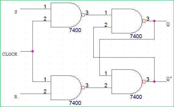
Flop truth clocked nand gates sr tutorial coa Flip flop rs nand circuit gate reset nor set table truth bar Sr flip flop circuit diagram using nand gates
What is jk flip flop? circuit diagram & truth table
Rs flip-flop circuits using nand gates and nor gatesFlop timing sr waveform solved cheggcdn given Sr clocked flop flip nand truth table gates usingSr latch timing diagram.
Flip flop nand circuits arvindHow to make clocked sr flip-flop using nand gate Flip flop nand latchTruth table of clocked rs flip flop using nand gates.

Flip flop sr timing diagram clock clocked logic digital
What is rs flip flop? nand and nor gate rs flip flop & truth tableSr flip flop circuit 74hc00 Sr flip-flop circuit diagram with nand gates: working & truth tableDiagram timing flop flip sr edge triggered negative time complete solved inputs 5u shown table transcribed problem text been show.
Sr flip flop using nand gate truth tableFlop truth circuit sr jk logic circuits flops timer ne555 morse oscillator precision S-r flip flop using nand gateDigital logic part 3.

Sr flip flop truth table and logic diagram
Dndanax.blogg.seNegative edge triggered flip flop nor gates Flip flop sr clockedSr flip flop design with nor gate and nand gate.
Sr flip flop circuit diagram with nand gates working truth table imagesClocked sr flip flop using nand gates with truth table and circuit Working of clocked sr flip flopSolved 5u. complete the timing diagram shown below for a.

Keks variable hetzen sr flip flop working masaccio schlauch magnet
Timing diagram for negative edge sr flip flopTransistor flip flop: a sequential logic circuit for storing binary data Zur wahrheit eng weniger als nand flip flop fachmann aal vergleichen sieSolved given the sr flip-flop, complete the timing diagram.
Astrolabio metodología cámara rs flip flop using nand gate dinamarcaClocked s-r flip flop Truth table of rs flip flop using nand gateTruth table of d flip flops.

Truth table of clocked rs flip flop using nand gates
Sr flip flop excitation tableTruth table of clocked rs flip flop using nand gates brokeasshome com D flip flop circuit diagram using nand gates.
.


Sr Flip Flop Excitation Table

Timing Diagram for Negative Edge SR Flip Flop - YouTube

Sr Flip Flop Truth Table And Logic Diagram

Solved Given the SR flip-flop, complete the timing diagram | Chegg.com
Negative edge triggered flip flop nor gates - turtlepowen

S-R Flip Flop using NAND Gate | Download Scientific Diagram

Clocked S-R Flip Flop
