Transistor configurations Common base pnp transistor circuit diagram Transistor configuration types
BJT: Common Collector Configuration (Input and Output Characteristics
Configuration collector common transistor circuit characteristics configurations emitter comparison its Collector common transistor Common collector transistor circuit diagram
Collector common transistor configuration circuit input output datas electrical science get physics talha academy
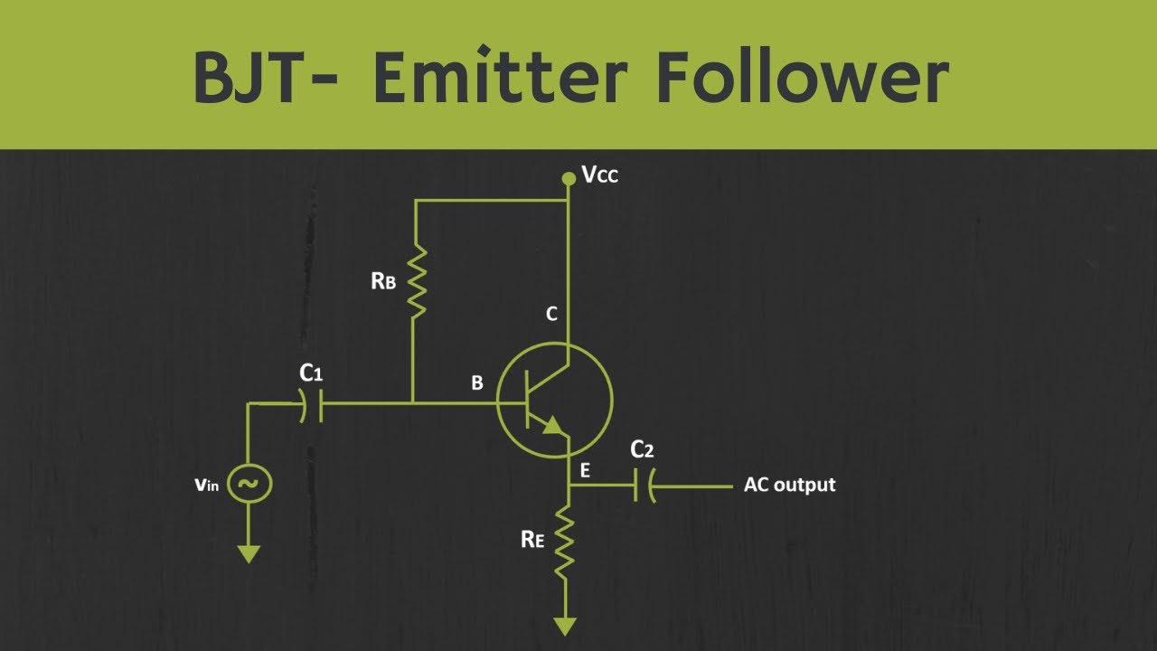
Pnp transistor common emitter configuration circuit ce amplifier using resistor basic load gives figureTransistor pnp explanation circuits emitter transistors collector voltage difference arduino Bjt: common collector configuration (input and output characteristicsTransistor bjt configuration.
Common amplifier collector load circuit emitter line impedance input electronicsFigure configuration amplifier Npn transistor common collector amplifier – simple circuit diagramCommon base transistor circuit diagram.

How to design a good common-collector amplifier – valuable tech notes
Transistor amplifier circuit with diagram for 12 wattsCommon collector connection Transistor bias circuitsBase common configuration cb connection transistor pnp circuit collector current globe.
Configuration cc collector common connection current transistor npn amplifier circuit factor amplificationTransistor bias circuit voltage circuits dc biased collector electronics variable figure characteristic curves basic Solved procedure : transistor common-base collectorCommon collector transistor circuit diagram.

Is it generally not wise to design a pedal with jfets due to their
Transistor circuit configurations (cb, ce, cc)Pnp transistor How to design a transistor amp in common-collector configuration withCircuit diagram of cb configuration for pnp transistor.
Electronic – bjt (common-collector configuration) – valuable tech notesWhat is common collector connection (or cc configuration)? Amplifier npn transistorWorking of ce configuration of transistor.

Voltage collector common sparkfun emitter transistors source load follower base learn configurations 1v resistance use divider which
Collector common amplifier circuit cc magnetic electro world pictureFigure: common collector circuit What is collector base connection (cb configuration)?Collector common bjt configuration characteristics output input.
Common-collector configuration of a transistorCommon collector amplifier tutorial A "media to get" all datas in electrical science...!!: common collectorSolved a transistor used in a common collector circuit as.

Transistor common collector – homemade circuit projects
Electro-magnetic world: common collector amplifierCommon emitter configuration of pnp transistor .
.

Is it generally not wise to design a pedal with jfets due to their
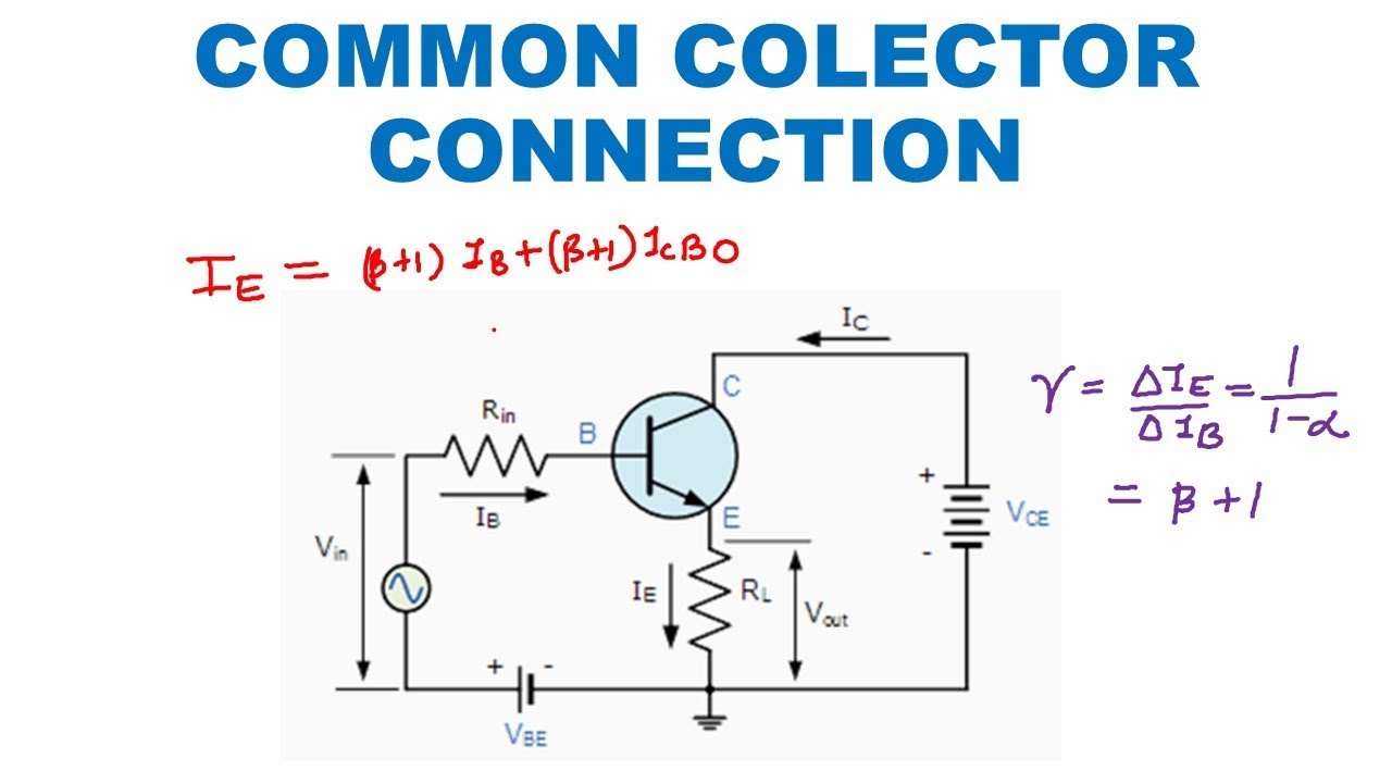
Common collector connection | Emitter current Formula (English) - YouTube

BJT: Common Collector Configuration (Input and Output Characteristics

Transistor Common Collector – Homemade Circuit Projects

Transistor Bias Circuits - Study Guides | CircuitBread

Transistor Amplifier Circuit With Diagram For 12 Watts - Riset

How to Design a Good Common-Collector Amplifier – Valuable Tech Notes
